Published on 03 February 2022

This short review shows the fabrication and characterisation of silicon-glass based microfluidic devices to be used in synchrotron facilities to measure toxic solutions using hard X-ray absorption spectroscopy, but also for acidic samples in (aq) solutions.
This short review article was based on the paper entitled “Fabrication and characterisation of a silicon-borosilicate glass microfluidic device for synchrotron-based hard X-ray spectroscopy studies” by Pushparani Micheal Raj, Laurent Barbe, Martin Andersson, Milena De Albuquerque Moreira, Dörthe Haase, James Wootton, Susan Nehzati, Ann E. Terry, Ross J. Friel, Maria Tenje and Kajsa G. V. Sigfridsson Clauss published in RSC Advances on 07 Sep 2021.
The paper shows first evidence of measuring K- and L- edges of iron, bromine and lead atom in aqueous solutions using smallest volumes of samples. This device was also tested with DMSO-based solutions which is toxic to handle and the microfluidic device was robust to withstand the solution for more than 24h.
Additionally, the flow sensors were used with the solutions without any damage and spillage.
ABSTRACT
A tri-layered glass-silicon based microfluidic device was tested on hard X-ray Absorption Spectroscopy at high intense Synchrotron facility at MAX IV – Sweden. The device was assessed for its suitability to continuously carry samples in solution. The samples were also toxic and acidic in nature. The device was integrated onto Balder beamline, X-ray spectroscopy was carried out on sample of FeCl3 (aq), NaBr, PbCl2 and PbAc2 flowing through. A comparison was done with a commerical off-the-shelf device flowing through the same samples to evaluate the performance.
The material was examined to be durable and robust against harsh solutions for more than 24 h of testing. The device substantiated to produce optimal spectral quality for low concentratiuon of samples as low as 100 mM. The device was tested and validated for K- and L- edges of several samples.
Watch the universal flow control webinar by Robin Oliveres that introduces microfluidic flow control!
INTRODUCTION
The study aimed to investigate the use of microfluidic chips that could be used for carrying sensitive samples in solution for X-ray analysis. Some samples such as proteins or highly valent transition metals are affected and damaged quickly by the beam and must be constantly refreshed. This is why a microfluidic chip was required to be used to flow samples in solution through. This would keep sample fresh but use as little volume as possible. A flow rate of 100µLmin−1 was the benchmark flow rate to avoid damage and consume a small amount of sample. It was necessary for the chip to meet some fundamental criteria. It must be easily manufactured and interfaced with the Balder beamline, where it was intended to be used. It must also be resistant to X-ray damage with minimal attenuation, and consume as little sample as possible while being able to refresh the sample quickly enough to avoid damage. Since the chip will likely be needed for analysis of hazardous samples such as Perovskites for solar cell research, it must be inert.
Any reaction with samples would be unacceptable. Lastly the chip must be interfaced with ElveFlow pressure controller and flow sensor, fitting in to a simple pressure driven flow set up arranged for the purposes of this investigation. In literature, studies provide a brief overview of the types of chips, and some chip production methods already used in the field [1].
Microfluidic chips have been used in X-ray absorption spectroscopy [2] but there is scope for further investigation of their usefulness and optimisation. It would be optimal to have chips with high aspect ratio channels (much deeper than they are wide) to allow for maximum X-ray exposure to the sample, while minimising the amount of sample consumed per experiment. Since the beam is very intense (in the order of 7000 eV and more, based on the atom of interest to be knocked out), it must be considered to what extent the beam damages the device material. Heat induced stressing of the chip, heat expansion/melting could be sources of deformation and subsequent failure and must be avoided. With these parameters in mind the material used to create the chip must be carefully selected so as not to interfere with the sample or X-ray data collection [3].
Much work has gone into designing and implementing these systems for experimental use on beamlines around the world [1]. The material, production technique and channel design of the chips were key parameters to the success of the project.
AIM & OBJECTIVES
The following objectives were defined:
-
Flow highly acidic and toxic solutions (aq) within microchannels
-
Measure the toxic solutions using hard X-ray Absorption Spectroscopy technique
-
Continuously refresh samples to avoid sample-beam interaction for a longer time
-
Have consistent flow rates to avoid any sample reduction due to high flux of energy used at beamlines in synchrotron facilities
MATERIALS & METHODS: Measuring solutions using hard X-ray absorption spectroscopy
Materials :
- Silicon wafer,
- borosilicate glass wafer,
- fused silica capillaries,
- PTFE tubing,
- Unions and connectors from Darwin Microfluidics.
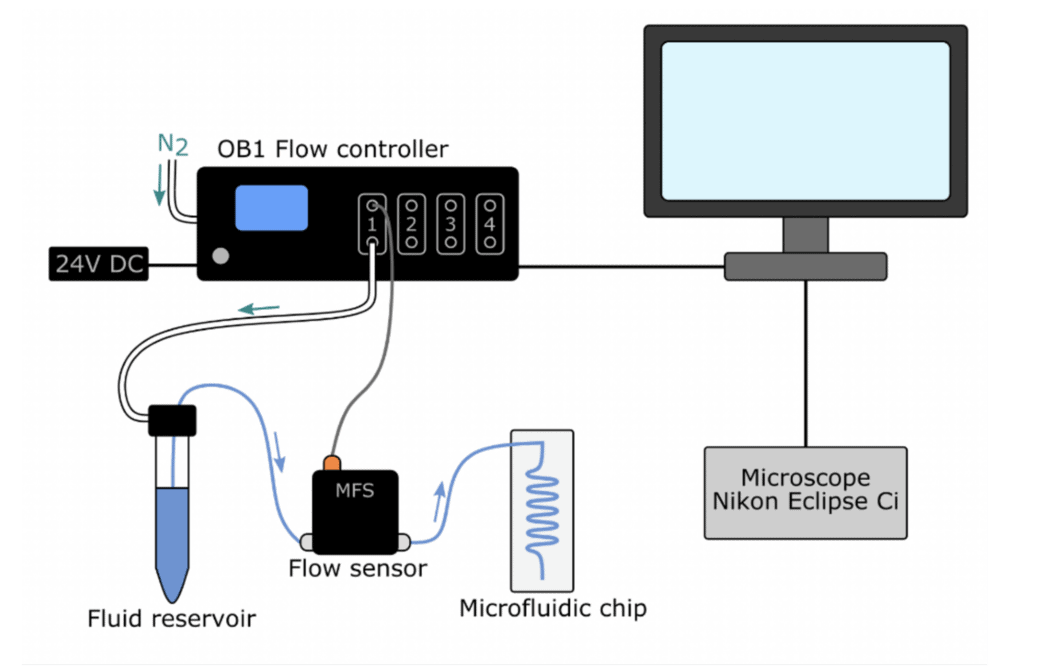
- Elveflow system – OB1 MK3+ Pressure controller, MFS microfluidic flow sensoRS.
The microfluidic device was fabricated using silicon wafers and borosilicate wafers, and employing lithography and anodic bonding of layers [4].
[starter_pack_rebound]
KEY FINDINGS: Measuring solutions using hard X-ray absorption spectroscopy
Microfluidic device fabrication & characterisation
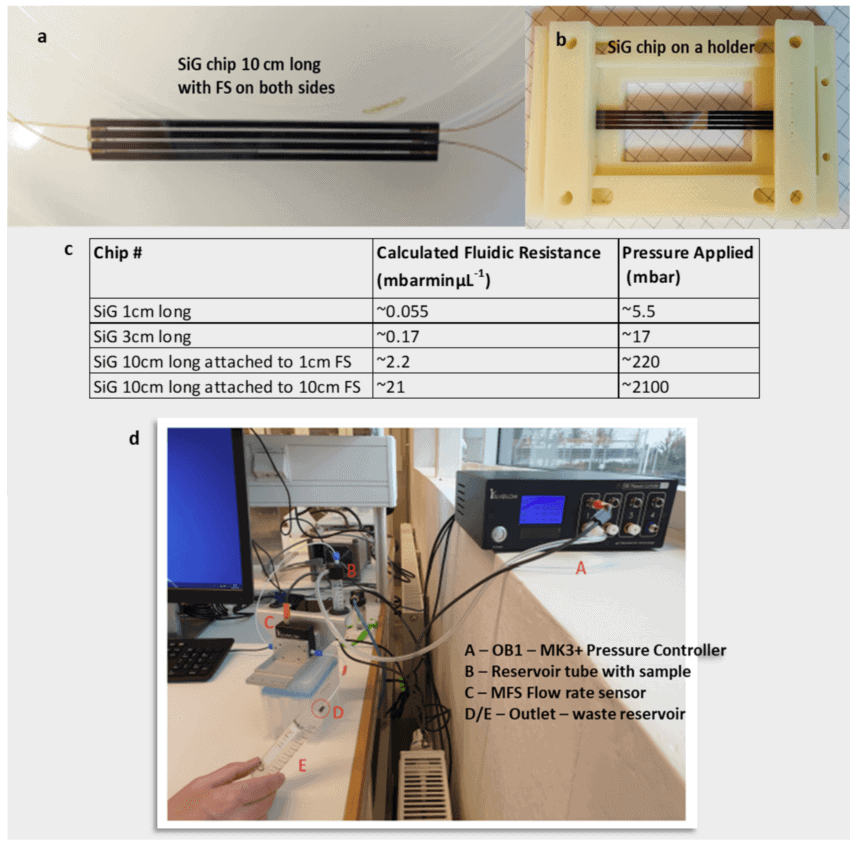
The silicon-borosilicate glass-silicon (SiG) wafer sandwiched microfluidic device was successfully fabricated with smooth channel walls using lithography and anodic bonding techniques [5]. The material was quite robust to withstand the high intense beams focusing at a single spot for more than 24 h. Additionally, the sample – material interaction was also conducive as expected. It was also observed that the channel with the fused silica capillary at different lengths produced favorable fluidic resistances that could be applied according to the viscosity of the samples.
Experimental setup
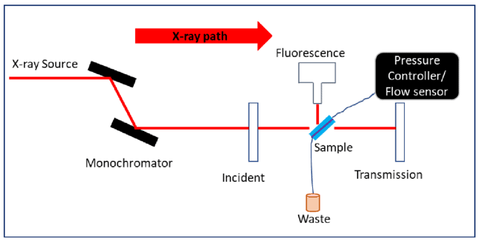
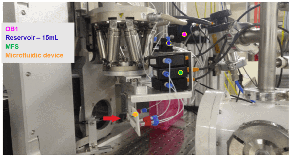
The microfluidic device was mounted on the beamline stage as in the picture below. A holder was machined to hold the flow sensors on the hexapod stage so as to provide a robust design throughout the experimental duration. The pressure system provided sufficient consistency to collect data with minimal sample volume and little manual intervention once the reservoir was fully loaded with sensitive and acidic samples. It is also important to note that the experiment was only remotely controlled as there is no entry possible into the experimental hutch in the beamlines during high X-ray beam experiments. Hence, the device was expected to be robust in design along with the peripherals like pressure controller and flow sensors to be remotely controlled. The SiG device was used for more than 24 h and data were collected in both transmission and fluorescence mode with the same device for samples of different concentrations.
Post-experimental setup
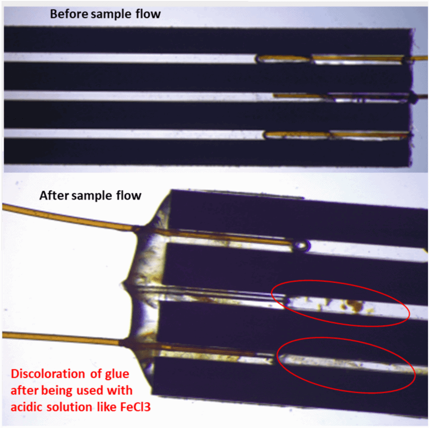
The most critical evaluation in the study was the beam-material interaction, the device was evaluated post-experiment. There was no apparent damage to the device itself that stops the reuse of the device. However, from the picture below, one could easily identify the discoloration of the glue when used with acidic samples like FeCl3 and NaBr. This is partly due to ageing of the device for more than 24 h and using multiple samples on the same device. This, then evinces that the device could be used with the similar samples again when thoroughly washed.
Data analysis
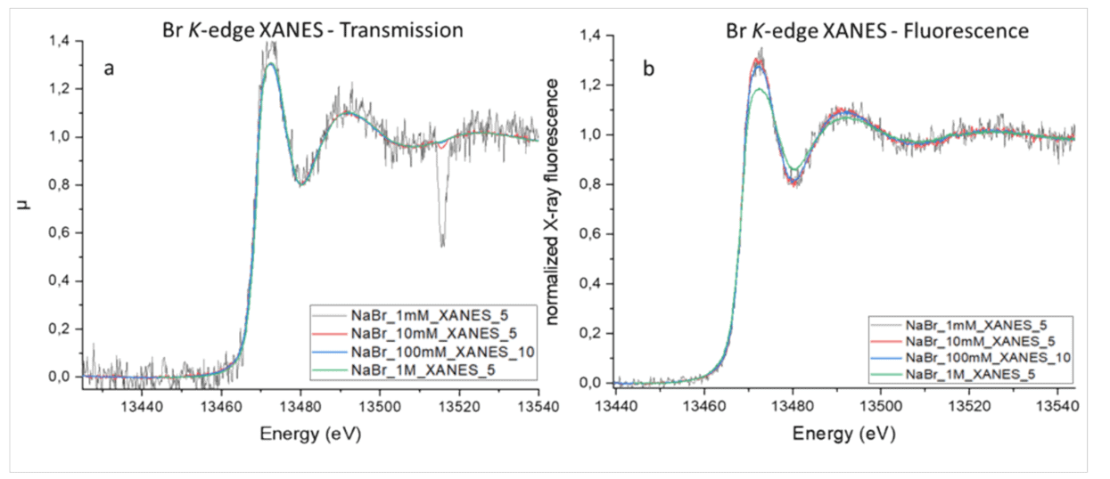
Several tests were carried out with different concentrations of FeCl3 and NaBr solutions (aq). A 100 mM concentration solution of FeCl3 (aq) at a rate of ∼ 10 µLmin−1 was flown. In order to compare and validate the presence of samples in the SiG chip, edges (pre-edges, K-edge and oscillatory tail) were determined and hence proved [3, 6]. Additionally, the features were analysed at lower concentrations to determine the attenuation characteristics of the material against X-ray beams. From physical and experimental validation post-flow, it is observed that the borosilicate windows act as a good window material for X-ray studies, however low concentrations as 1 mM provided low signal to noise ratio.
The SiG device was tested in transmission and fluorescence modes of detection to assess the quality of spectra obtained. It is observed that the SiG device performed equally well in both modes. Spectra from both modes of measurement are exhibited in the pictures below.
CONCLUSION
The SiG microfluidic device presented in this paper allowed a continuous XAS analysis of liquid samples using X-ray beams of higher energies (good for 7 keV and optimal mostly above 13 keV). The device fabrication was rapid and customizable to obtain multiple channels in a single chip resulting in high throughput. The device was quantified over a long time (>24 h) and demonstrated to work well in typical of synchrotron-based hard XAS experiments.
The device and fabrication method has manifested to be optimal for sensitive samples and high intense energy beams. There is no reduction of samples on the channel walls, thus providing an ideal environment to measure solutions using micro volumes of samples and yet using the most sensitive analytical technique like X-ray spectroscopy.
References
- Ghazal, A., et al., Recent advances in X-ray compatible microfluidics for applications in soft materials and life sciences. Lab Chip, 2016. 16(22): p. 4263-4295.
- Chan, E.M., et al., Millisecond kinetics of nanocrystal cation exchange using microfluidic X-ray absorption spectroscopy. J Phys Chem A, 2007. 111(49): p. 12210-5.
- Reschke, S., et al., Identification of a bis-molybdopterin intermediate in molybdenum cofactor biosynthesis in Escherichia coli. J Biol Chem, 2013. 288(41): p. 29736-45.
- Beuvier, T., et al., Implementation of in situ SAXS/WAXS characterization into silicon/glass microreactors. Lab Chip, 2015. 15(9): p. 2002-8.
- Ari, J., et al., Anodic bonding of mid-infrared transparent germanate glasses for high pressure – high temperature microfluidic applications. Sci Technol Adv Mater, 2020. 21(1): p. 11-24.
- Ankudinov, A.L. and J.J.J.P.R.B. Rehr, RELATIVISTIC CALCULATIONS OF SPIN-DEPENDENT X-RAY-ABSORPTION SPECTRA. 1997. 56: p. 1712-1715.

 Job
Job Collaborations
 Customer
 Other
Other