Introduction to Photomasks in Microfluidics
What is a Photolithography Mask?

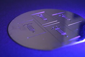
A photolithography mask is an opaque plate or film with transparent areas which allows light to shine through a defined pattern. They are commonly used in photolithography processes, but are also used in many other applications by a wide range of industries and technologies, notably microfluidics.
The photolithography mask acts as a template, and is designed to optically transfer patterns onto wafers or other substrates in order to fabricate devices of all types.
There are three types of basic material used to make photolithography masks:

Soda Lime (SL), Quartz, and polyester film.
Soda Lime and quartz are the most common substrates for photolithography masks, and typical glass mask sizes can range from 3 square inches to 7 square inches.
Film photolithography masks have less constraints on size, and can be made on sheets from 25 cm x 30 cm (10” x 12”) , up to a huge 3 m long x 1 m wide (120” x 40”). The polyester base on the film is 0.18 mm thick.
| Quartz | Soda Lime | Plastic mask |
|
Expensive High resolution Very stable Can break Wavelength >180nm |
Good price/quality ratio High resolution Easy to clean Stable Can break Wavelength >350nm |
Low price Low resolution Weak stability Easy to handle Wavelength >350nm |
Using negative photoresist, the unexposed, or masked, portion of this material is then removed. So, the remaining photoresist can form channels mold for microfluidic applications or protect the underneath substrate so the non-covered substrate parts can be etched.
Photolithography masks are used in wafer fabrication, microfluidics, strain gauges, MEMS, Optics, flat panel displays, BioMed, PC boards…. but are also used in many other applications by a wide range of industries and technologies.
Where are photolithography masks used?
FULL SOFT-LITHO BOX
A turnkey offer to fabricate your su-8 mold and pdms chips
How are photolithography masks used?
Photolithography masks are used in various applications and processes, but one of the most common procedures is to use the mask in a ‘mask aligner’.
One of the most important step in the photolithography process is the mask alignment. The photolithography mask is aligned with the wafer, so that the pattern can be transferred onto the wafer surface. Many MEMS devices are made with multiple materials and multiple layers, so in that case each mask after the first one must be aligned to the previous pattern for the device to work correctly.
Sometimes the alignment between these layers is highly critical and a complex expensive machinery is required.
Once the photolithography mask has been accurately aligned with the pattern on the wafer’s surface, the photoresist is exposed through the pattern on the mask with a high intensity ultraviolet light.
There are three primary exposure methods: contact, proximity, and projection.
Contact Printing
In contact printing, the resist-coated silicon wafer (or other substrate) is brought into physical contact with the glass photolithography mask. The wafer is held on a vacuum chuck, and the whole assembly rises until the wafer and mask contact each other.
The photoresist is exposed to UV light while the wafer is in contact position with the photolithography mask. Because of the contact between the resist and mask, very high resolution is possible in contact printing (e.g. 1-micron features in 0.5 microns of positive resist).
The problem with contact printing is that debris, trapped between the resist and the photolithography mask can damage the mask and cause defects in the pattern.
Proximity Printing
The proximity exposure method is similar to contact printing except that a small gap, 10 to 25 microns wide, is maintained between the wafer and the mask during the exposure. This gap minimizes (but may not eliminate) wafer damage. Approximately 2- to 4-micron resolution is possible with proximity printing.
Projection Printing
Projection printing avoids mask damage entirely. An image of the patterns on the photolithography mask is projected onto the resist-coated wafer, which is many centimeters away. In order to achieve high resolution, only a small portion of the photolithography mask is imaged. This small image field is scanned or stepped over the surface of the wafer.
Projection printers that step the mask image over the wafer surface are called step-and-repeat systems. Step-and-repeat projection printers are capable of approximately 1-micron resolution.
For more information or Technical discussion

Microfluidics knowledge
Do you want tips on how to best set up your microfluidic experiment? Do you need inspiration or a different angle to take on your specific problem? Well, we probably have an application note just for you, feel free to check them out!


 Job
Job Collaborations
 Customer
 Other
Other